 plumi
Discrete semiconductor devices: AQA A‑Level Physics questions
Every AQA A-Level Physics exam question on 3.13.1 Discrete semiconductor devices, 2016–2025, with its mark scheme and examiner’s report.
Find questions2,714
Calculations
Q03.1
The whole paper ↗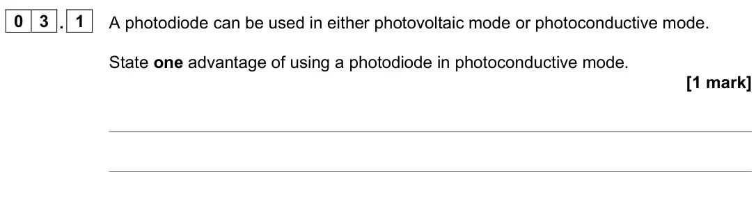
Q04.1
The whole paper ↗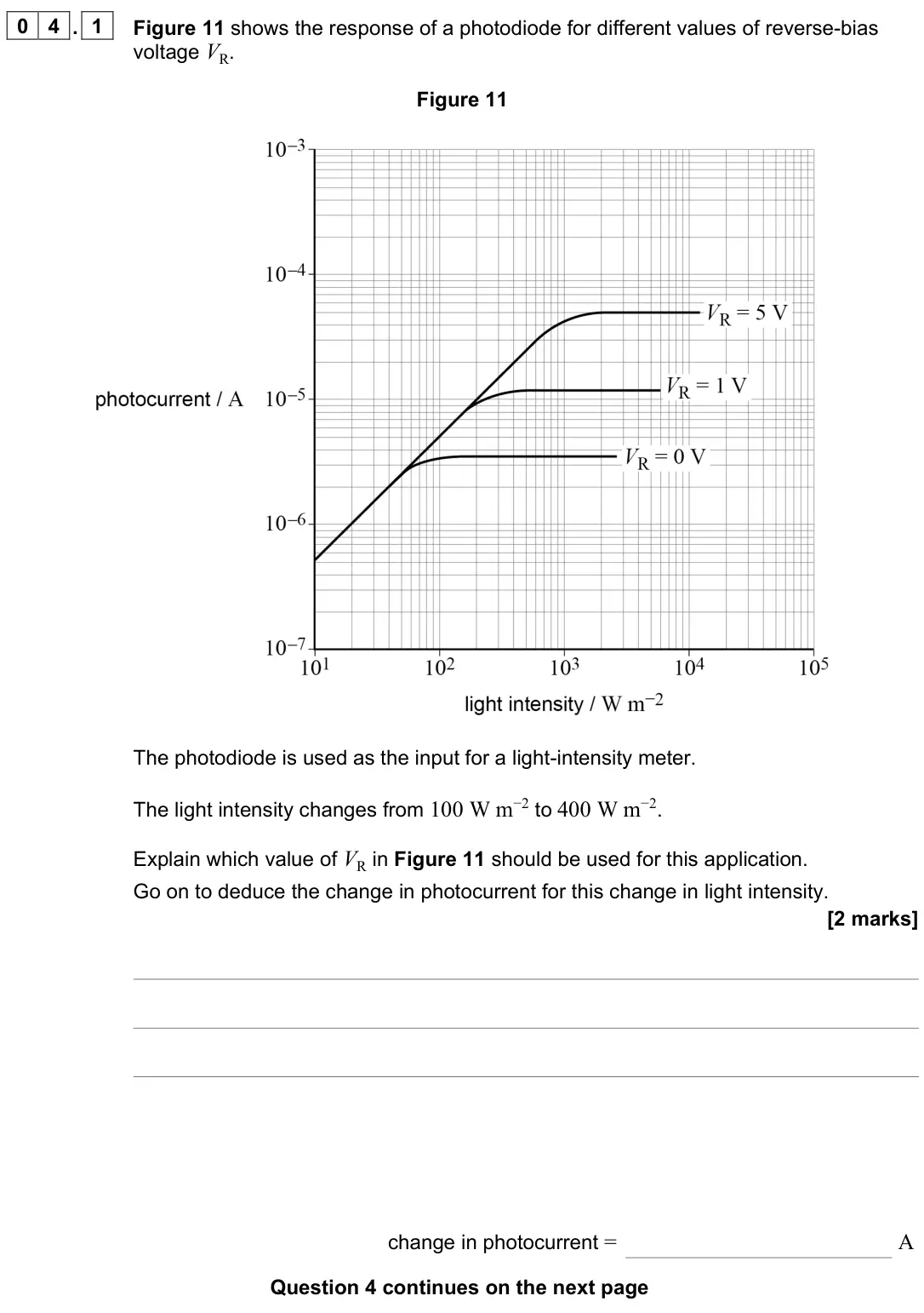
Q04.2
The whole paper ↗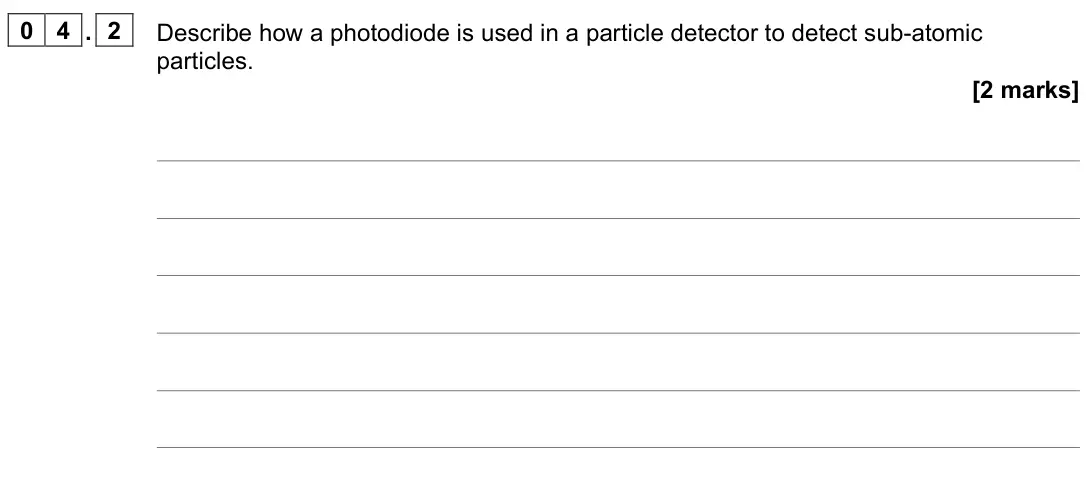
Q02.1
The whole paper ↗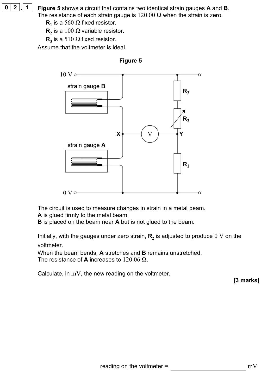
Q02.2
The whole paper ↗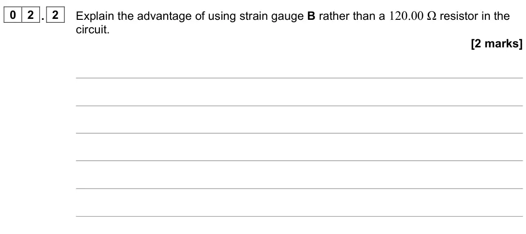
Q01.1
The whole paper ↗
Q01.2
The whole paper ↗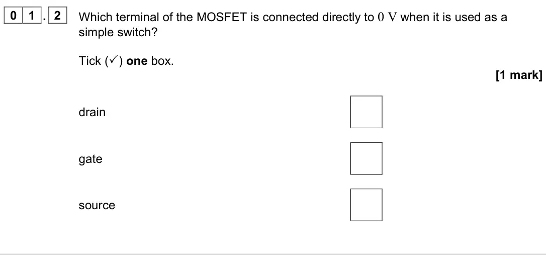
Q01.3
The whole paper ↗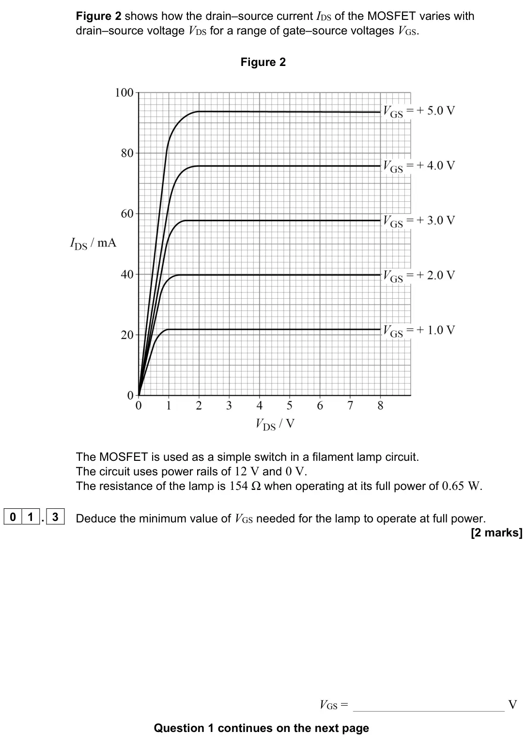
Q01.4
The whole paper ↗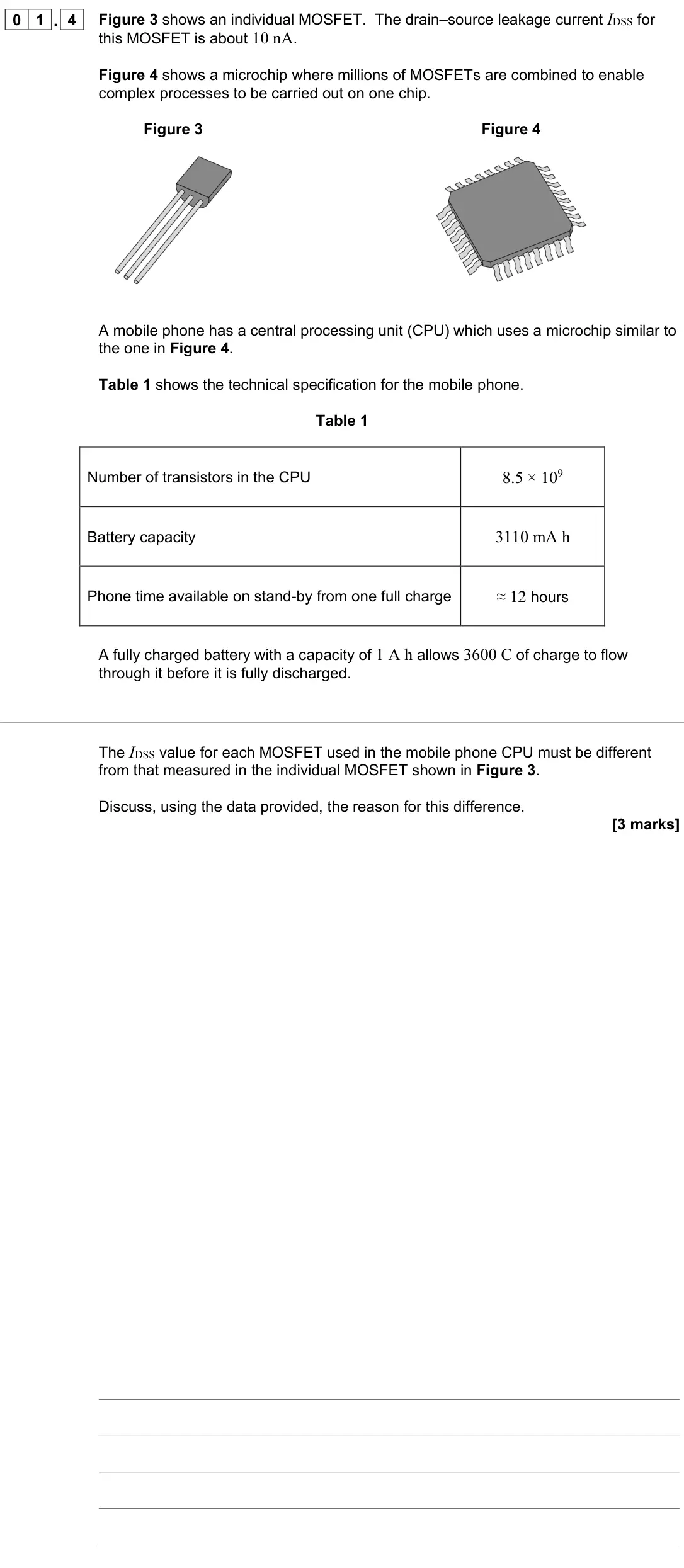
Q03.1
The whole paper ↗
Q03.2
The whole paper ↗
Q03.3
The whole paper ↗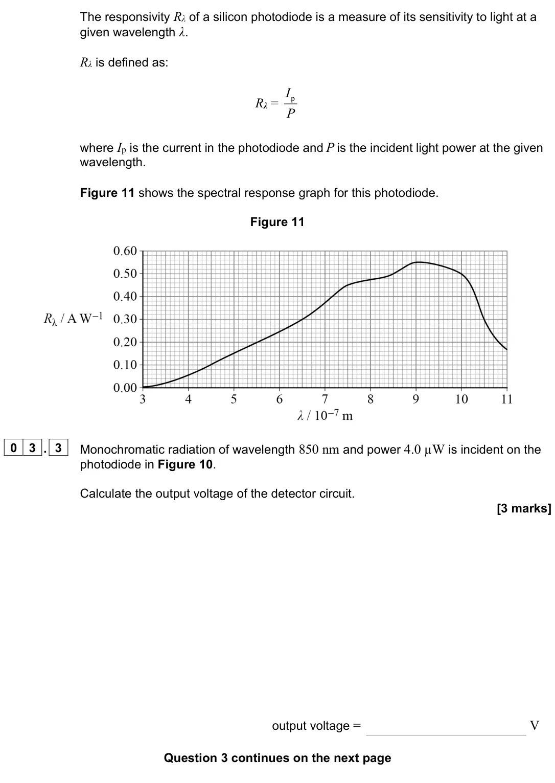
Q01.4
The whole paper ↗
Q03.1
The whole paper ↗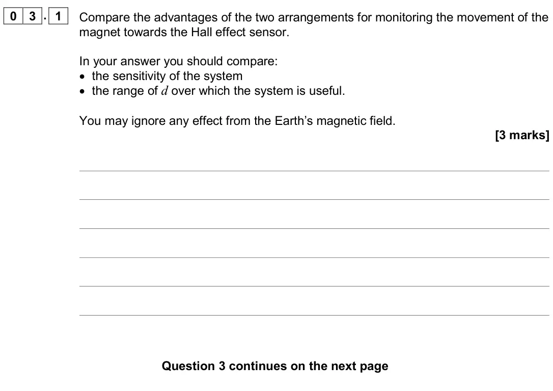
Q04.1
The whole paper ↗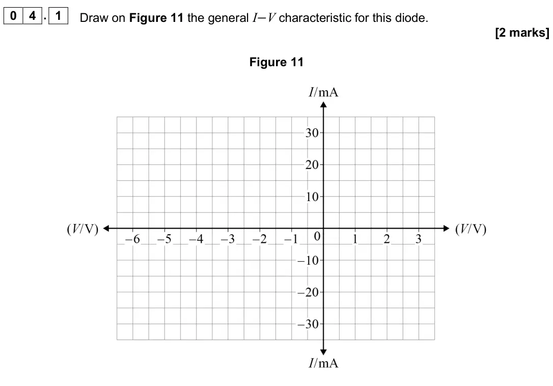
Q04.2
The whole paper ↗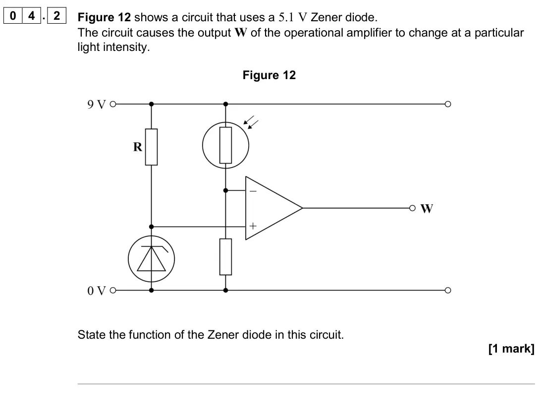
Q04.3
The whole paper ↗
Q04.4
The whole paper ↗
All 27 questions on Discrete semiconductor devices, as a list
- June 2025, Paper 3 Electronics, Q03.1 (1 mark): A photodiode can be used in either photovoltaic mode or photoconductive mode. State one advantage of using a photodiode in photoconductive mode. [1 mark]
- June 2024, Paper 3 Electronics, Q04.1 (2 marks): Figure 11 shows the response of a photodiode for different values of reverse-bias voltage VR. Figure 11 The photodiode is used as the input for a light-intensit
- June 2024, Paper 3 Electronics, Q04.2 (2 marks): Describe how a photodiode is used in a particle detector to detect sub-atomic particles. [2 marks]
- June 2023, Paper 3 Electronics, Q02.1 (3 marks): Figure 5 shows a circuit that contains two identical strain gauges A and B. The resistance of each strain gauge is 120.00 Ω when the strain is zero. R1 is a 560
- June 2023, Paper 3 Electronics, Q02.2 (2 marks): Explain the advantage of using strain gauge B rather than a 120.00 Ω resistor in the circuit. [2 marks]
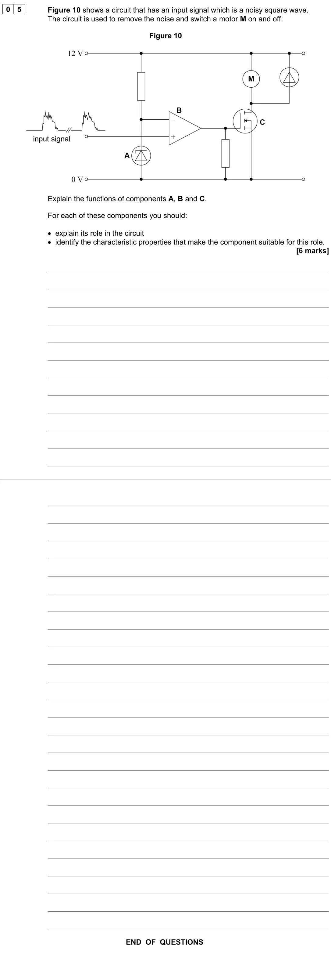
- June 2023, Paper 3 Electronics, Q05 (6 marks): Figure 10 shows a circuit that has an input signal which is a noisy square wave. The circuit is used to remove the noise and switch a motor M on and off. Figure
- November 2021, Paper 3 Electronics, Q01.1 (1 mark): State the name of the part shown in this MOSFET structure that causes the input resistance to be very large. [1 mark]
- November 2021, Paper 3 Electronics, Q01.2 (1 mark): Which terminal of the MOSFET is connected directly to 0 V when it is used as a simple switch? Tick () one box. [1 mark] drain gate source
- November 2021, Paper 3 Electronics, Q01.3 (2 marks): Deduce the minimum value of VGS needed for the lamp to operate at full power. [2 marks] VGS = V
- November 2021, Paper 3 Electronics, Q01.4 (3 marks): Figure 3 shows an individual MOSFET. The drain–source leakage current IDSS for this MOSFET is about 10 nA. Figure 4 shows a microchip where millions of MOSFETs
- November 2021, Paper 3 Electronics, Q03.1 (1 mark): State the mode in which the photodiode is being used in Figure 10. [1 mark]
- November 2021, Paper 3 Electronics, Q03.2 (1 mark): In the circuit shown in Figure 10, there is a current in the photodiode even when there is no light incident on it. This current is called the dark current. In
- November 2021, Paper 3 Electronics, Q03.3 (3 marks): Monochromatic radiation of wavelength 850 nm and power 4.0 µW is incident on the photodiode in Figure 10. Calculate the output voltage of the detector circuit.
- June 2019, Paper 3 Electronics, Q01.4 (3 marks): The potential difference across the green LED is 2.1 V when it is lit. The current through it should not exceed 9 mA. All logic gate outputs are: logic low = 0
- June 2019, Paper 3 Electronics, Q03.1 (3 marks): Compare the advantages of the two arrangements for monitoring the movement of the magnet towards the Hall effect sensor. In your answer you should compare: • th
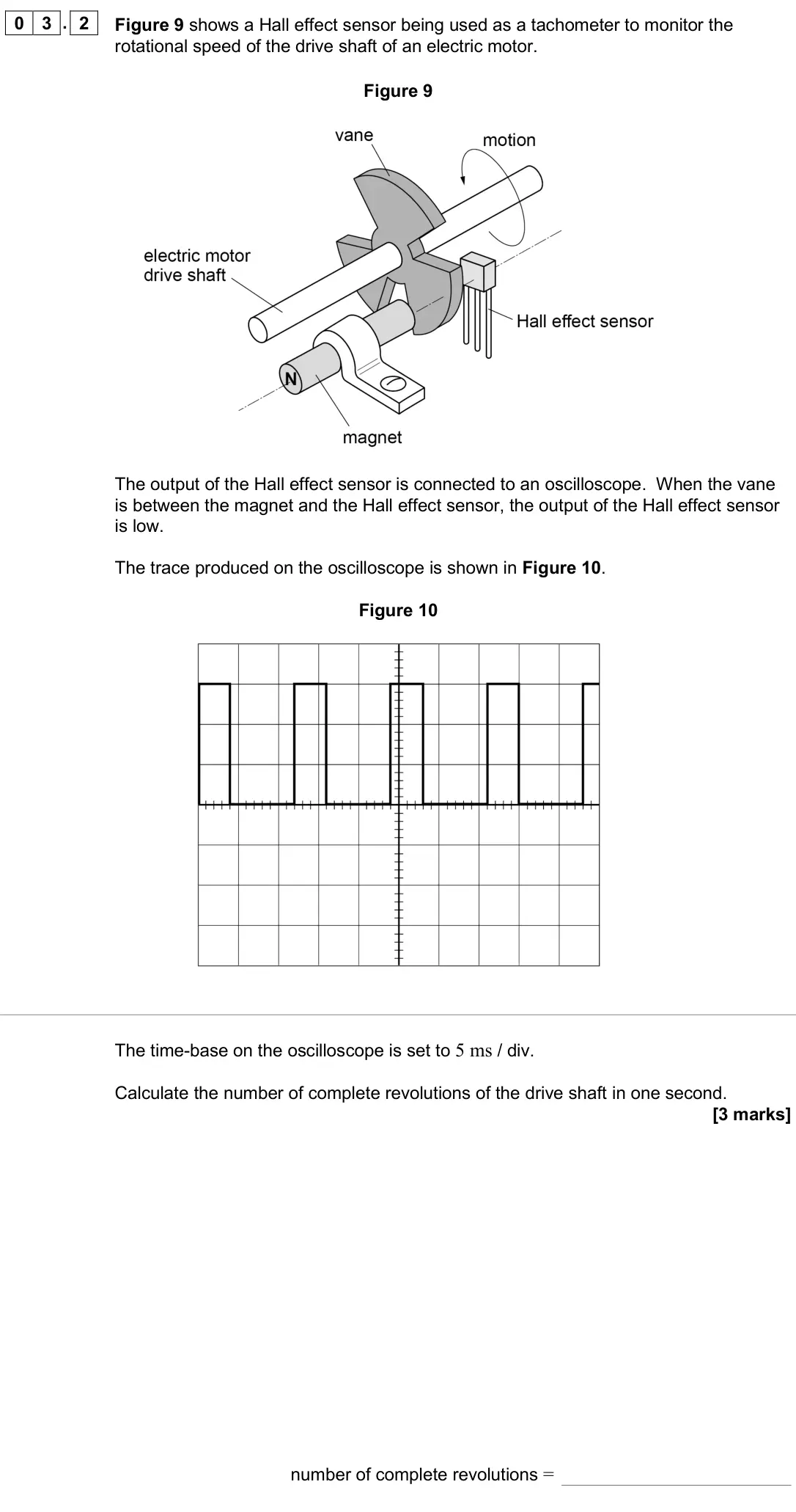
- June 2019, Paper 3 Electronics, Q03.2 (3 marks): Figure 9 shows a Hall effect sensor being used as a tachometer to monitor the rotational speed of the drive shaft of an electric motor. Figure 9 The output of t
- June 2019, Paper 3 Electronics, Q04.1 (2 marks): Draw on Figure 11 the general I−V characteristic for this diode. [2 marks] Figure 11
- June 2019, Paper 3 Electronics, Q04.2 (1 mark): Figure 12 shows a circuit that uses a 5.1 V Zener diode. The circuit causes the output W of the operational amplifier to change at a particular light intensity.
- June 2019, Paper 3 Electronics, Q04.3 (2 marks): Deduce whether a 100 Ω, 0.13 W resistor is suitable for R in Figure 12. [2 marks]
- June 2019, Paper 3 Electronics, Q04.4 (2 marks): The circuit in Figure 12 is rebuilt and the position of R is swapped with the position of the Zener diode. Explain how this affects the light intensity at which
- June 2019, Paper 3 Electronics, Q04.6 (1 mark): Output Q from Figure 13 becomes the input to the final part of the circuit shown in Figure 14. Figure 14 The circuit uses a MOSFET to activate a relay. State on
- June 2017, Paper 3 Electronics, Q04.1 (1 mark): State the mode in which the photodiode is being used in Figure 10. [1 mark]
- June 2017, Paper 3 Electronics, Q04.3 (1 mark): Figure 11 shows an extract from a data sheet of the characteristics for a photodiode under different light levels measured in lux. For a particular lighting con
- June 2017, Paper 3 Electronics, Q04.4 (1 mark): Calculate the voltage at point X in the circuit shown in Figure 10 for the light level in question 04.3. [1 mark] voltage = V
- Specimen, Paper 3 Electronics, Q01.1 (2 marks): MOSFETs are commonly used in circuits where low power consumption is important to extend battery life. State and explain the property of MOSFET devices that mak
- Specimen, Paper 3 Electronics, Q01.2 (2 marks): Figure 1 shows an N-channel enhancement mode MOSFET, being used as part of a circuit for the water level alarm in a garden pond. When the gap between the copper
- Specimen, Paper 3 Electronics, Q01.3 (2 marks): The circuit is tested by immersing the copper strips in the water, and bringing them closer together until the alarm sounds. Vth for the MOSFET in Figure 1 is 2
Questions, mark schemes and examiner’s reports are © AQA, from their published past papers. Plumi isn’t affiliated with any exam board. Want whole papers? Every AQA A-Level Physics paper.
Rather write your answers by hand on iPad? Plumi marks them against the same mark schemes.