 plumi
Digital signal processing: AQA A‑Level Physics questions
Every AQA A-Level Physics exam question on 3.13.5 Digital signal processing, 2016–2025, with its mark scheme and examiner’s report.
Find questions2,714
Calculations
Q01.1
The whole paper ↗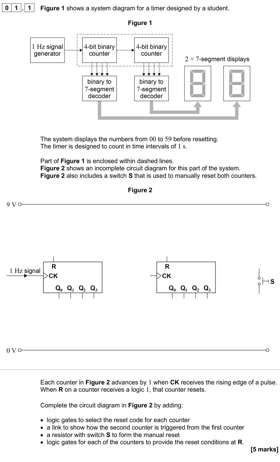
Q01.2
The whole paper ↗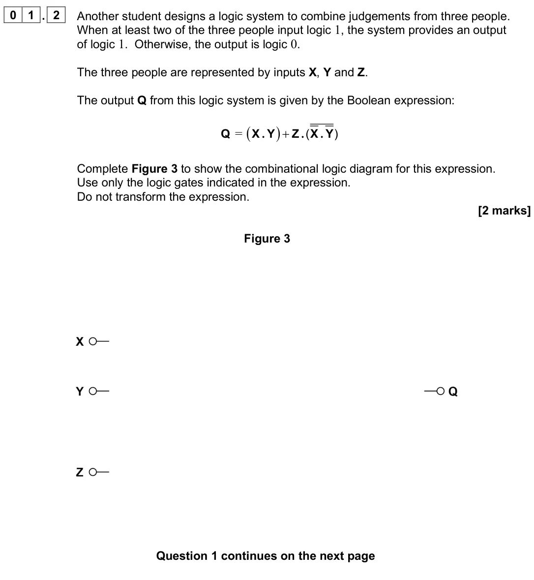
Q01.3
The whole paper ↗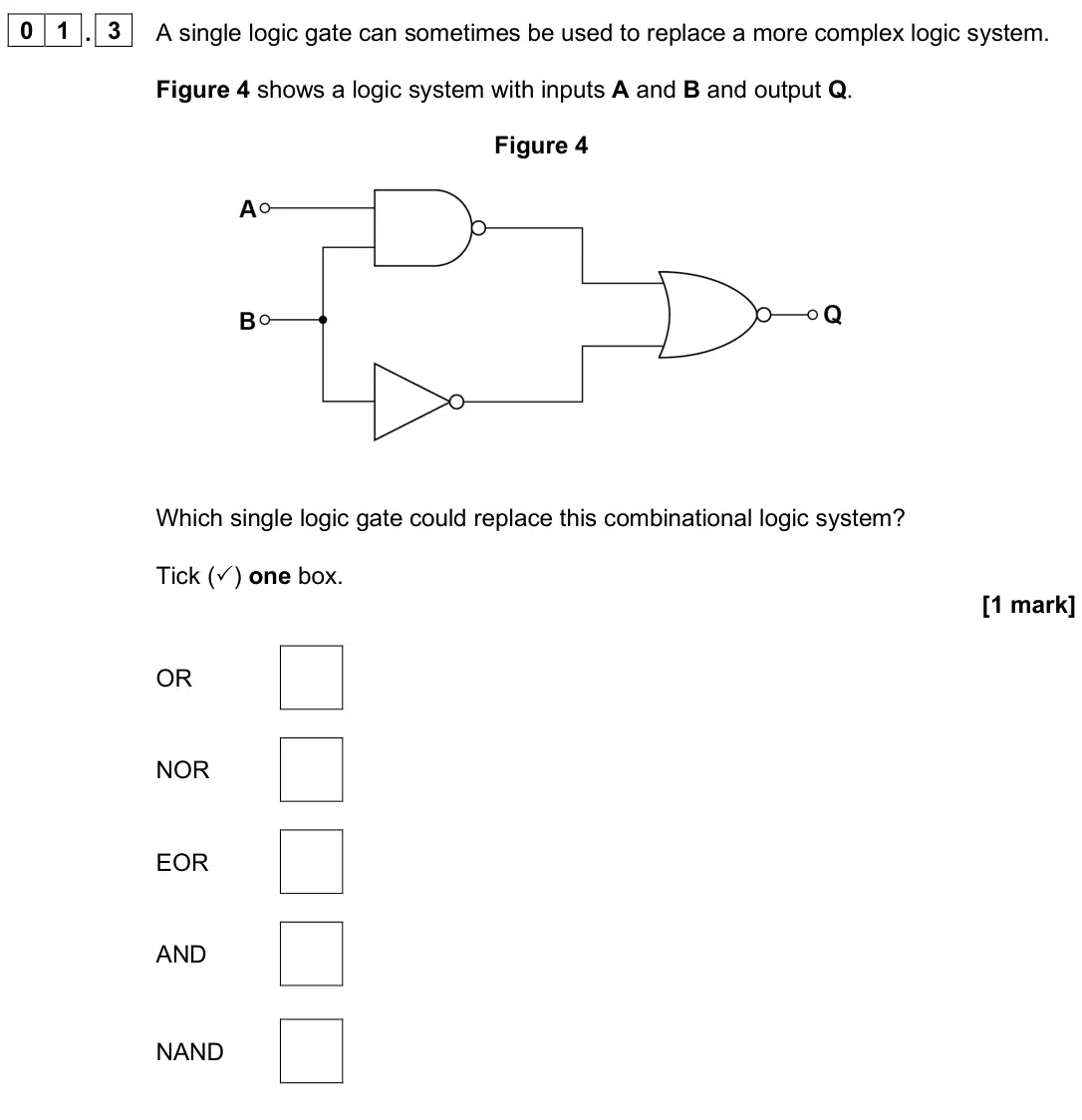
Q02.4
The whole paper ↗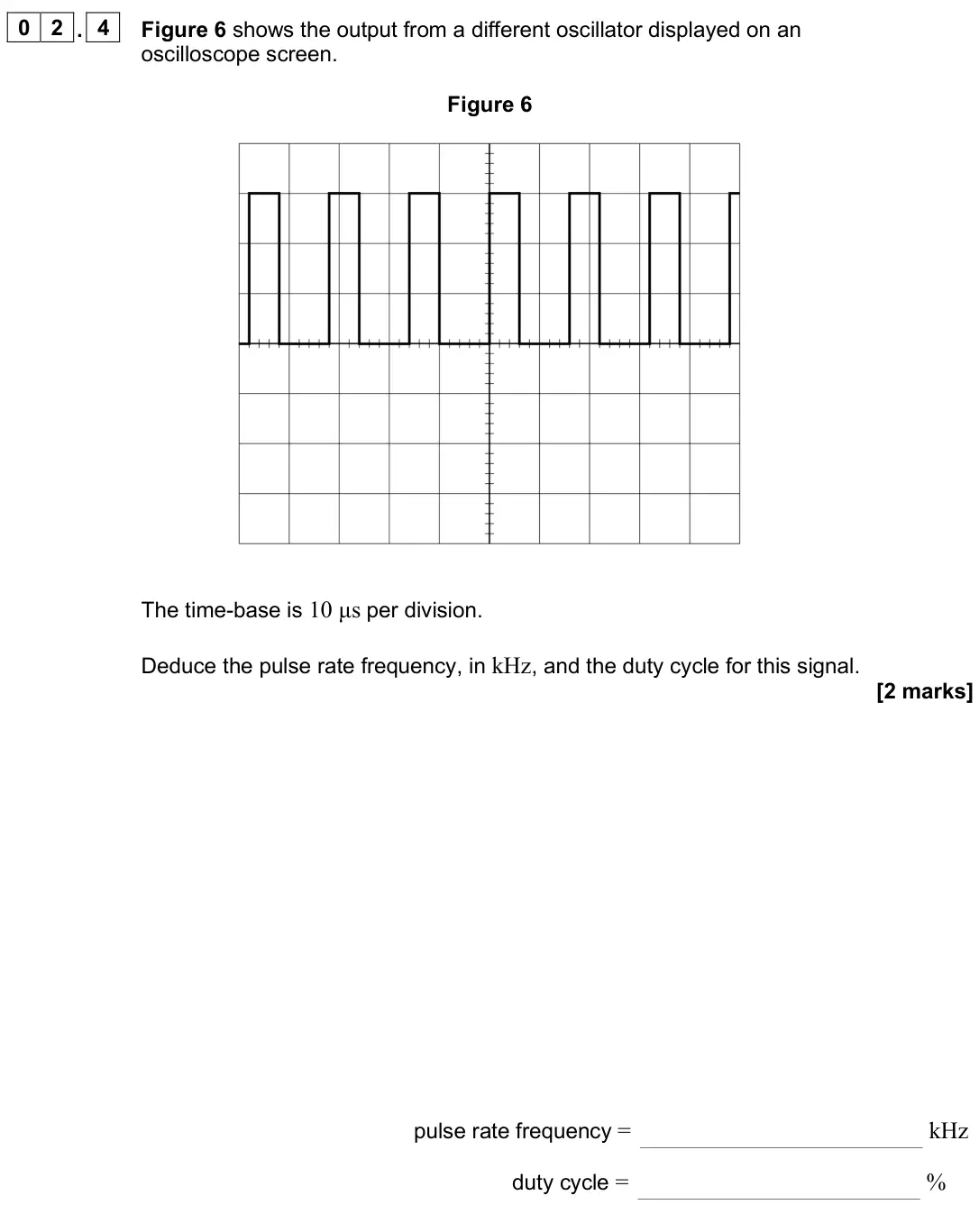
Q01.1
The whole paper ↗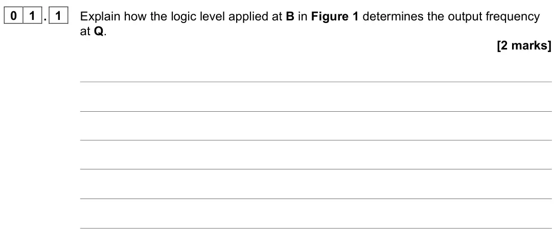
Q01.2
The whole paper ↗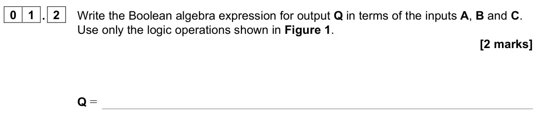
Q01.3
The whole paper ↗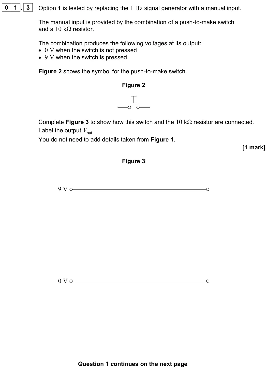
Q01.4
The whole paper ↗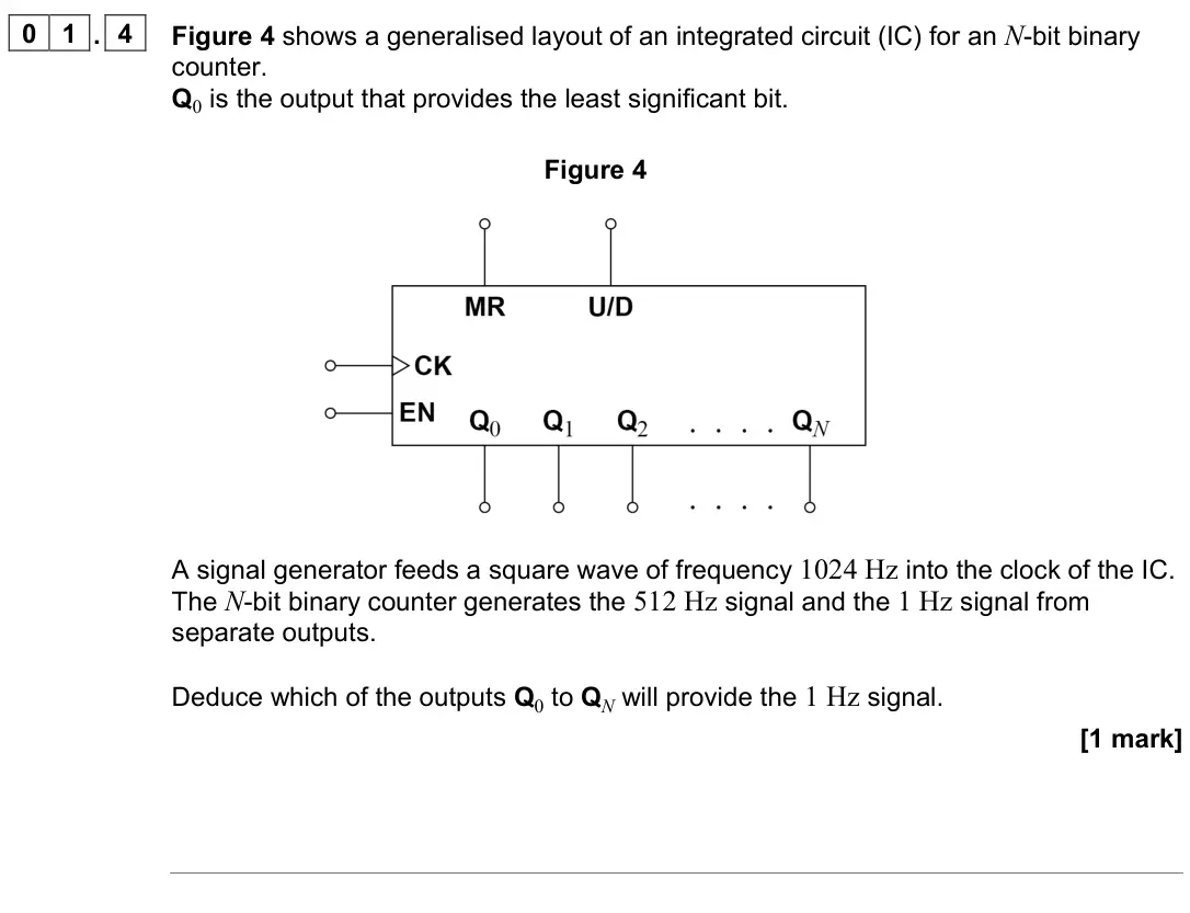
Q01.5
The whole paper ↗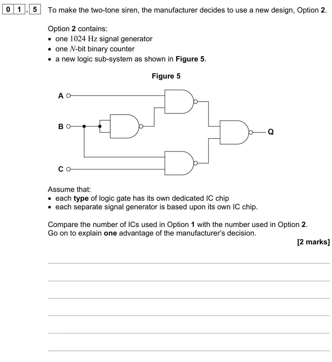
Q02.4
The whole paper ↗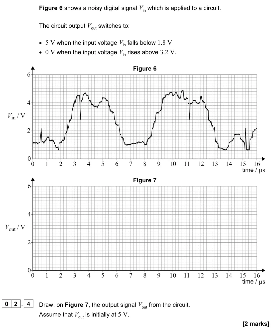
Q01.1
The whole paper ↗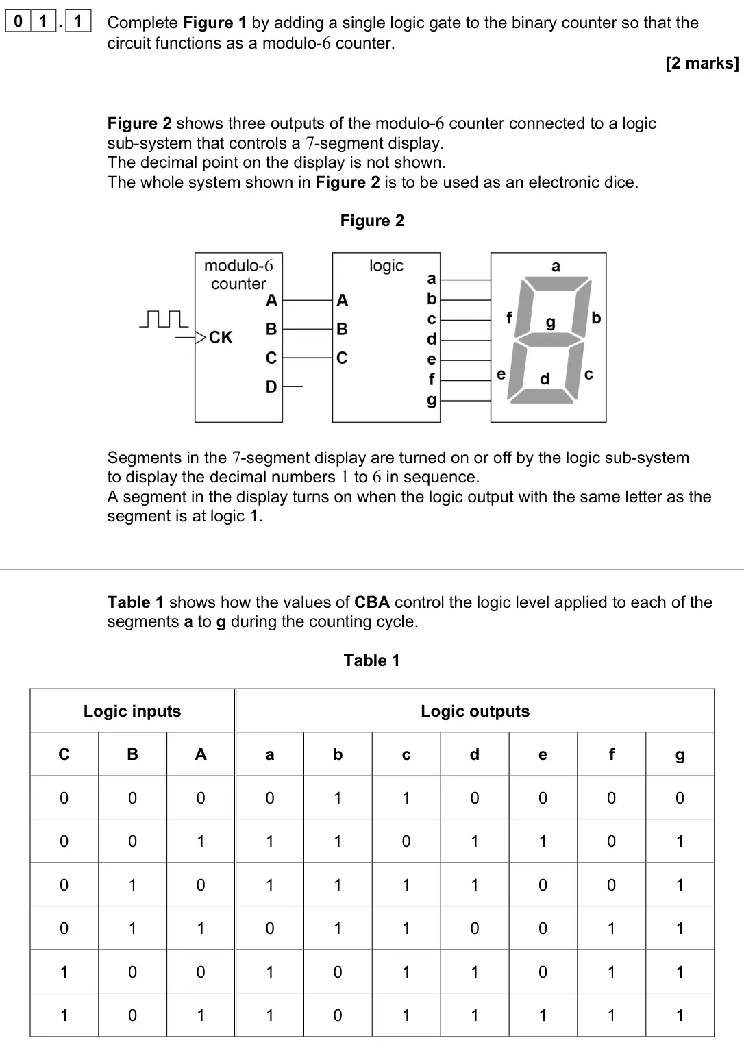
Q01.2
The whole paper ↗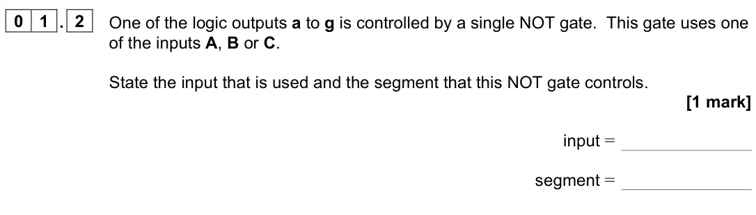
Q01.3
The whole paper ↗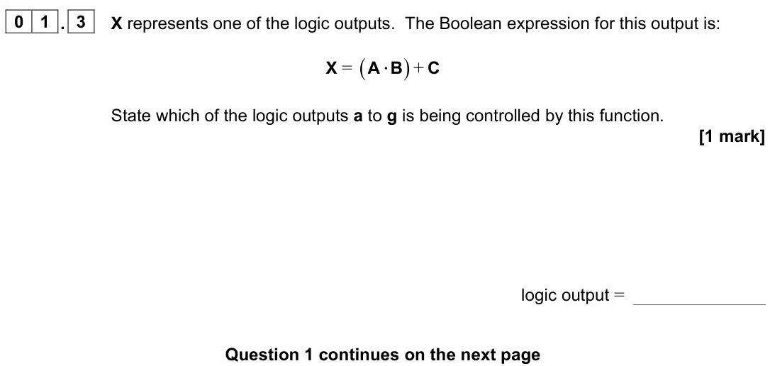
Q01.4
The whole paper ↗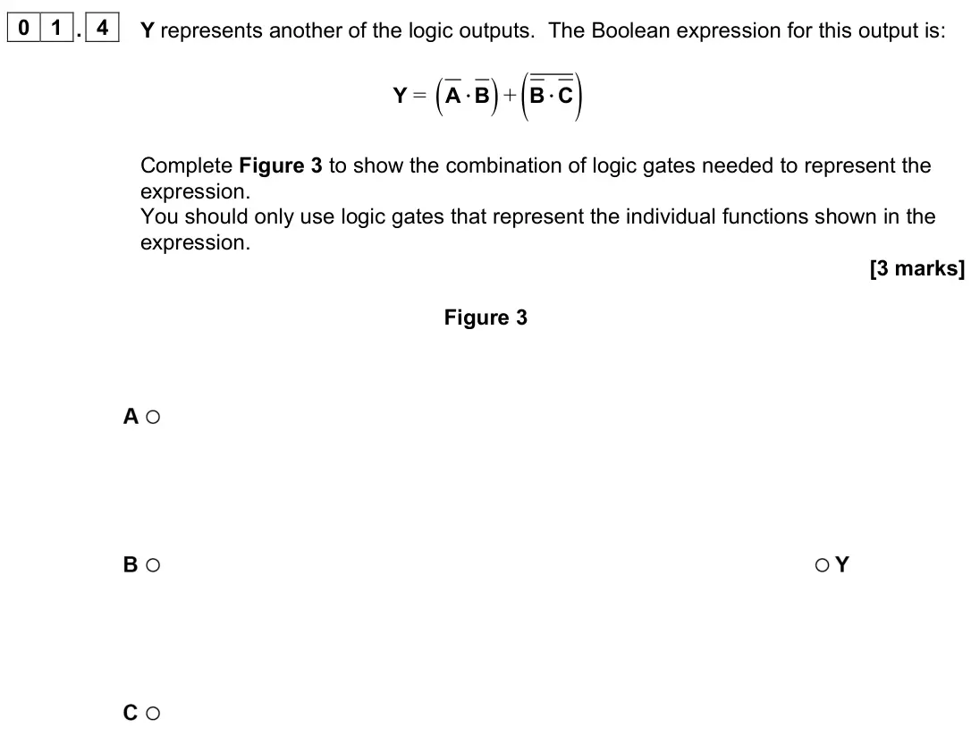
Q02.1
The whole paper ↗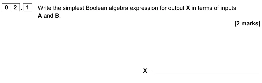
Q02.2
The whole paper ↗
Q02.3
The whole paper ↗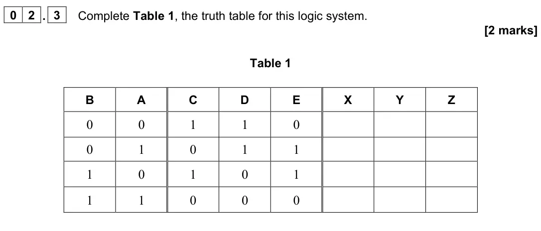
Q02.4
The whole paper ↗
Q02.5
The whole paper ↗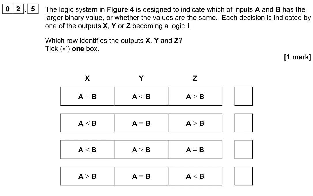
All 54 questions on Digital signal processing, as a list
- June 2025, Paper 3 Electronics, Q01.1 (5 marks): Figure 1 shows a system diagram for a timer designed by a student. Figure 1 The system displays the numbers from 00 to 59 before resetting. The timer is designe
- June 2025, Paper 3 Electronics, Q01.2 (2 marks): Another student designs a logic system to combine judgements from three people. When at least two of the three people input logic 1, the system provides an outp
- June 2025, Paper 3 Electronics, Q01.3 (1 mark): A single logic gate can sometimes be used to replace a more complex logic system. Figure 4 shows a logic system with inputs A and B and output Q. Figure 4 Which
- June 2025, Paper 3 Electronics, Q02.4 (2 marks): Figure 6 shows the output from a different oscillator displayed on an oscilloscope screen. Figure 6 The time-base is 10 μs per division. Deduce the pulse rate f
- June 2024, Paper 3 Electronics, Q01.1 (2 marks): Explain how the logic level applied at B in Figure 1 determines the output frequency at Q. [2 marks]
- June 2024, Paper 3 Electronics, Q01.2 (2 marks): Write the Boolean algebra expression for output Q in terms of the inputs A, B and C. Use only the logic operations shown in Figure 1. [2 marks] Q =
- June 2024, Paper 3 Electronics, Q01.3 (1 mark): Option 1 is tested by replacing the 1 Hz signal generator with a manual input. The manual input is provided by the combination of a push-to-make switch and a 10
- June 2024, Paper 3 Electronics, Q01.4 (1 mark): Figure 4 shows a generalised layout of an integrated circuit (IC) for an N-bit binary counter. Q0 is the output that provides the least significant bit. Figure
- June 2024, Paper 3 Electronics, Q01.5 (2 marks): To make the two-tone siren, the manufacturer decides to use a new design, Option 2. Option 2 contains: • one 1024 Hz signal generator • one N-bit binary counter
- June 2024, Paper 3 Electronics, Q02.4 (2 marks): Draw, on Figure 7, the output signal Vout from the circuit. Assume that Vout is initially at 5 V. [2 marks]
- June 2023, Paper 3 Electronics, Q01.1 (2 marks): Complete Figure 1 by adding a single logic gate to the binary counter so that the circuit functions as a modulo-6 counter. [2 marks] Figure 2 shows three output
- June 2023, Paper 3 Electronics, Q01.2 (1 mark): One of the logic outputs a to g is controlled by a single NOT gate. This gate uses one of the inputs A, B or C. State the input that is used and the segment tha
- June 2023, Paper 3 Electronics, Q01.3 (1 mark): X represents one of the logic outputs. The Boolean expression for this output is: X = ( ) + ⋅ A B C State which of the logic outputs a to g is being controlled
- June 2023, Paper 3 Electronics, Q01.4 (3 marks): Y represents another of the logic outputs. The Boolean expression for this output is: Y = ( ) ( ) + ⋅ ⋅ A B B C Complete Figure 3 to show the combination of log
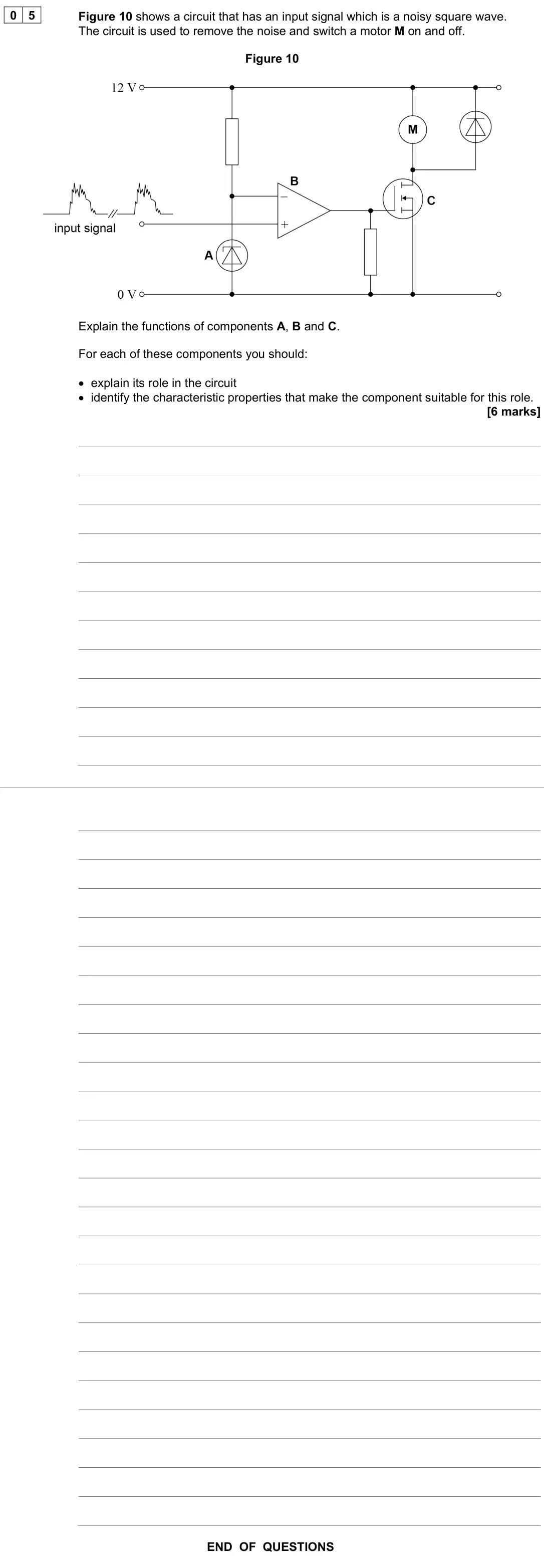
- June 2023, Paper 3 Electronics, Q05 (6 marks): Figure 10 shows a circuit that has an input signal which is a noisy square wave. The circuit is used to remove the noise and switch a motor M on and off. Figure
- June 2022, Paper 3 Electronics, Q02.1 (2 marks): Write the simplest Boolean algebra expression for output X in terms of inputs A and B. [2 marks] X =
- June 2022, Paper 3 Electronics, Q02.2 (1 mark): State the name of logic gate 5 in Figure 4. [1 mark]
- June 2022, Paper 3 Electronics, Q02.3 (2 marks): Complete Table 1, the truth table for this logic system. [2 marks] Table 1 B A C D E X Y Z 0 0 1 1 0 0 1 0 1 1 1 0 1 0 1 1 1 0 0 0
- June 2022, Paper 3 Electronics, Q02.4 (1 mark): Suggest a single logic gate that can replace the combination of gates 5 and 6 in this system. [1 mark]
- June 2022, Paper 3 Electronics, Q02.5 (1 mark): The logic system in Figure 4 is designed to indicate which of inputs A and B has the larger binary value, or whether the values are the same. Each decision is i
- June 2022, Paper 3 Electronics, Q04.1 (3 marks): Initially the capacitor is uncharged and Vc is at 0 V. Explain the sequence of actions of this circuit as the output goes through one full cycle. The first two
- June 2022, Paper 3 Electronics, Q04.2 (4 marks): Figure 7 shows the oscillator circuit after it has been modified by the addition of: • two diodes D1 and D2 • a potential divider that has a total resistance va
- November 2021, Paper 3 Electronics, Q02.1 (1 mark): Table 2 is a partially completed truth table for the logic subsystem. Table 2 Inputs Output C B A Q 0 0 0 0 0 0 1 0 0 1 0 0 0 1 1 0 1 0 0 1 1 0 1 1 1 0 1 1 1 Co
- November 2021, Paper 3 Electronics, Q02.2 (2 marks): Complete Figure 7 to show how this switch, together with a 10 kΩ resistor, can be connected to create the door detector circuit in Figure 5. Label the output of
- November 2021, Paper 3 Electronics, Q02.3 (2 marks): Write the Boolean algebra expression for Q in terms of inputs A, B and C. In your answer use only AND and NOR operators. [2 marks] Q =
- November 2021, Paper 3 Electronics, Q02.4 (1 mark): Figure 9 shows a logic circuit that has the same function as the circuit in Figure 8. Only one type of gate is used in the circuit in Figure 9. Figure 9 State t
- November 2021, Paper 3 Electronics, Q02.5 (1 mark): Microchips containing two-input logic gates are mass-produced. Each microchip contains four identical logic gates. A manufacturer of the logic circuit used in t
- November 2021, Paper 3 Electronics, Q04.1 (2 marks): Describe one functional difference and one functional similarity between how a Johnson decade counter and a BCD counter output their counts. [2 marks] functiona
- November 2021, Paper 3 Electronics, Q04.2 (3 marks): An astable oscillator produces a continuous train of pulses. Figure 13 shows the display of the pulses on an oscilloscope. Figure 13 The oscilloscope settings a
- November 2021, Paper 3 Electronics, Q04.3 (2 marks): The astable is adjusted to produce a 600 Hz test signal. This signal is applied to the clock input of the BCD counter and to the clock input of the Johnson deca
- November 2020, Paper 3 Electronics, Q01.1 (3 marks): Complete Figure 1 to show how both reset conditions can be met. Do not show the power line connections to the integrated circuit. [3 marks]
- November 2020, Paper 3 Electronics, Q01.2 (2 marks): A logic system is designed to identify prime numbers. The binary codes from the counter are now applied to the inputs ABC of the logic system shown in Figure 2.
- November 2020, Paper 3 Electronics, Q01.3 (1 mark): Complete Table 1, the truth table for the logic system in Figure 2. [1 mark] Table 1 Decimal number C B A D E F W 0 0 0 0 1 0 0 1 0 0 1 1 0 0 2 0 1 0 1 0 1 3 0
- November 2020, Paper 3 Electronics, Q01.4 (1 mark): The logic system in Question 01.2 is replaced with one that gives an output S using the same binary input codes CBA. The Boolean algebra equation for output S i
- November 2020, Paper 3 Electronics, Q01.5 (2 marks): Complete Figure 3 by drawing the logic system for S. You must use only the logic gate operations given in S = + A B C .( ) [2 marks] Figure 3
- June 2019, Paper 3 Electronics, Q01.1 (2 marks): Figure 2 shows part of the timing diagram for a Johnson decade counter. This timing diagram shows the output logic states against time. The counter is reset to
- June 2019, Paper 3 Electronics, Q01.2 (1 mark): A student sets up the counter to make the traffic light sequence: red → red + amber → green → amber The sequence then repeats. Figure 3 shows a partially comple
- June 2019, Paper 3 Electronics, Q01.3 (2 marks): State two factors that determine the ON time for the green LED shown in Figure 3. [2 marks] 1 2
- June 2019, Paper 3 Electronics, Q04.5 (1 mark): The output W from the operational amplifier shown in Figure 12 becomes one of three inputs to the combinational logic circuit shown in Figure 13. Figure 13 Writ
- June 2018, Paper 3 Electronics, Q01.1 (2 marks): Two logic inputs, A and B, feed into the logic circuit shown in Figure 1. The logic output from the circuit is Q. Figure 1 Deduce the Boolean expression for the
- June 2018, Paper 3 Electronics, Q01.2 (2 marks): The truth table shows some of the logic states for the logic gates in Figure 1. Complete the truth table. [2 marks] B A C D E F Q 0 0 1 0 0 0 1 1 1 1 1 0 0 0 1
- June 2018, Paper 3 Electronics, Q01.3 (2 marks): Figure 2 shows a different logic circuit that produces the same logic output as that of Figure 1. Figure 2 A manufacturer wants to produce a system that uses th
- June 2018, Paper 3 Electronics, Q01.4 (1 mark): State the single logic gate that would perform the same logic function as the circuits shown in Figure 1 and Figure 2. [1 mark]
- June 2018, Paper 3 Electronics, Q04.1 (1 mark): Figure 6 shows an astable circuit based on a NOT logic gate. The symbol in the centre of the logic gate means that the output Vo changes at two different input
- June 2018, Paper 3 Electronics, Q04.2 (1 mark): The supply voltage to the NOT gate is Vs • When Vc increases and reaches the upper switching threshold (UST), the output of the NOT gate will switch from Vs to
- June 2018, Paper 3 Electronics, Q04.3 (2 marks): The circuit in Figure 6 can be modified by the addition of a resistor to vary the PRF. The astable is to be modified so that it produces a frequency 4 times tha
- June 2018, Paper 3 Electronics, Q04.4 (2 marks): In another astable, two resistors (R1 and R2) and a capacitor C form a timing chain to control the mark and space times for a square wave produced at the output
- June 2018, Paper 3 Electronics, Q04.5 (2 marks): The output of the IC in Figure 8 is 5 V during the charging period and 0 V during the discharging period. Draw on Figure 9 the wave pattern that represents this
- June 2017, Paper 3 Electronics, Q02.1 (2 marks): Complete Table 1 to show the logic outputs for the lamps L1 and L6. [2 marks]
- June 2017, Paper 3 Electronics, Q02.2 (1 mark): Deduce the simplest Boolean expression that can be used to show how output L7 can be controlled by the logic inputs. [1 mark]
- June 2017, Paper 3 Electronics, Q02.3 (2 marks): Figure 6 shows some of the input and output pins of the 4-bit binary counter. The data sheet for the counter indicates that the counter resets when the reset pi
- June 2017, Paper 3 Electronics, Q02.4 (3 marks): The output of both L3 and L4 can be written as (A . B . Cഥ) + (Bഥ . C) Figure 7 shows part of a logic circuit needed to represent this Boolean expression. Compl
- Specimen, Paper 3 Electronics, Q06.1 (1 mark): The Boolean equation for a particular logic circuit with inputs A and B and output Q is: 𝐐= (𝐀. 𝐁) + (𝐀ഥ. 𝐁ഥ) 0 6 Table 1 shows intermediate logic signals for t
- Specimen, Paper 3 Electronics, Q06.2 (3 marks): The Boolean equation for a particular logic circuit with inputs A and B and output Q is: 𝐐= (𝐀. 𝐁) + (𝐀ഥ. 𝐁ഥ) 0 6 Complete the diagram in Figure 6 to show the l
Questions, mark schemes and examiner’s reports are © AQA, from their published past papers. Plumi isn’t affiliated with any exam board. Want whole papers? Every AQA A-Level Physics paper.
Rather write your answers by hand on iPad? Plumi marks them against the same mark schemes.